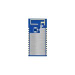
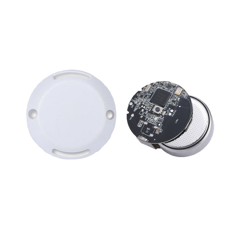
The antenna is the single most critical element determining a BLE tag‘s effective range, power consumption, and positional stability. In form factors under 40 mm, every millimeter of ground plane, every dielectric boundary, and every housing material choice directly reshapes the radiation pattern. This article quantifies those trade-offs with measured data and provides design guidelines for engineers working on the next generation of compact asset-tracking tags.
Antenna Topology Selection for Small Tags
Three antenna types dominate sub-40 mm BLE tag designs. Each trades off bandwidth, efficiency, and PCB area differently:
| Type | Typical Size | Peak Efficiency | Bandwidth (S11 < -10 dB) | Ground Plane Req. |
|---|---|---|---|---|
| Meandered Inverted-F (MIFA) | 18 × 5 mm | 45-60% | 80-120 MHz | ≥ 20 mm |
| PIFA (Planar Inverted-F) | 10 × 10 mm | 35-50% | 60-90 MHz | ≥ 15 mm |
| Ceramic Chip (e.g. Johanson 2450AT18A100) | 3.2 × 1.6 mm | 20-35% | 150-250 MHz | Min (self-resonant) |
For coin-cell tags (CR2032/CR2450), the MIFA offers the best efficiency-to-area ratio. For ultra-compact key-fob form factors, the ceramic chip antenna eliminates layout complexity at the cost of 15-20 percentage points in efficiency. The PIFA sits in between and is preferred when the tag sits on a metallic surface—the shorting pin provides a natural return path that reduces detuning.
Ground Plane and Clearance Area Budget
In a 30 mm diameter circular tag, the available PCB area is ~707 mm². After allocating space for the SoC (nRF52832 QFN: 48 mm²), coin cell holder (~180 mm²), sensor ICs (~20 mm²), and passives (~40 mm²), the antenna + ground plane budget is roughly 420 mm². This constraint drives the following ground-plane rules:
- Minimum ground length: 20 mm (λ/6 at 2.45 GHz) for MIFA; below this, efficiency drops ~3 dB per 5 mm reduction
- Clearance above antenna: 5 mm minimum copper-free zone on all layers; dielectric-only (FR4 εr ≈ 4.4)
- Keep-out from battery: CR2032 creates a 20 mm metallic disk—maintain ≥ 3 mm lateral clearance or the antenna pattern tilts 15-25° toward the battery
- Via stitching: Ring the ground plane perimeter with vias on 1.5 mm pitch to suppress edge radiation and improve pattern symmetry
Impedance Matching Network Design
BLE SoCs present a complex output impedance that varies by part. The nRF52832 data sheet specifies Zout = (16.5 + j14.5) Ω at 2.44 GHz; the CC2640R2F specifies (30 + j15) Ω. Both require a matching network to transform to the antenna’s 50 Ω input.
A Pi-network (C1–L–C2) provides the most flexibility for production tuning:
- C1 (SoC side): 0.5–2.2 pF, NP0/C0G dielectric (±0.1 pF tolerance)
- L (series): 1.5–4.7 nH, wirewound (Q > 25 at 2.4 GHz)
- C2 (antenna side): 0.3–1.5 pF, NP0/C0G
Practical tip: layout all three footprints even if the final BOM uses only two components. This allows retuning in-production without a board spin. For MIFA antennas, the measured input impedance at the feed point typically ranges from 20–35 Ω with j10–j25 reactance; the Pi-network covers this entire range with standard E12 values.
Housing Material Effects on Resonant Frequency
The tag’s plastic housing acts as a dielectric overlay that shifts the antenna’s resonant frequency downward. The shift depends on material permittivity, wall thickness, and proximity to the radiating element:
| Housing Material | εr (2.4 GHz) | Wall Thickness (mm) | Freq. Shift (MHz) | Efficiency Loss (dB) |
|---|---|---|---|---|
| ABS | 2.7–3.0 | 1.5 | -40 to -60 | 0.5–1.0 |
| PC | 2.9–3.2 | 1.5 | -50 to -80 | 0.8–1.5 |
| PC/ABS blend | 2.8–3.1 | 1.5 | -45 to -70 | 0.6–1.2 |
| TPU (overmold) | 3.0–4.0 | 2.0 | -80 to -150 | 1.5–3.0 |
| Potted epoxy | 3.5–4.5 | Full encapsulation | -120 to -200 | 2.5–4.5 |
Design rule: tune the bare-board antenna 60–100 MHz high (2.50–2.54 GHz center) so the housing brings it back to 2.44 GHz. This “pre-detuning” approach is standard in production—measure each housing batch’s permittivity (using a parallel-plate fixture) and adjust C1/C2 accordingly. For IP67 potted tags, the -120 to -200 MHz shift requires aggressive pre-detuning plus a wider bandwidth topology (ceramic chip or meandered monopole with ground-truncation).
Human Body and Mounting Surface Effects
A BLE tag mounted on or near lossy dielectrics (human tissue, cardboard, liquid containers) experiences both detuning and absorption:
- Worn on body (lanyard/badge): efficiency drops 6–10 dB, pattern becomes hemispherical (away from body). Solution: place antenna on the outward-facing PCB edge, use a 3 mm foam spacer between tag and skin
- On metal shelf: if directly attached, the antenna is short-circuited; efficiency drops > 15 dB. Solution: 5 mm foam spacer or use a PIFA with ground-plane isolation
- On cardboard box: εr ≈ 1.5–2.0; minimal detuning but 1–2 dB efficiency loss from moisture absorption at high humidity
- Near liquids (warehouse with beverages): water’s εr ≈ 78 at 2.4 GHz causes severe detuning (> 200 MHz shift) and > 10 dB absorption within 10 mm
Radiation Pattern Optimization
For asset tracking in open warehouses, an omnidirectional pattern in the horizontal plane maximizes gateway detection probability. In a 30 mm tag, the MIFA radiates most strongly broadside to the PCB; the pattern has 4–6 dB nulls along the PCB edges. Two techniques improve pattern uniformity:
- Corner placement: Position the antenna at one corner of a rectangular PCB (e.g., 35 × 25 mm). The truncated ground plane creates a more uniform H-plane pattern with < 3 dB variation over 360°
- Ground-plane slot: A 2 mm wide L-shaped slot in the ground plane, 5 mm from the antenna feed, breaks up ground currents and reduces nulls by 2–3 dB
Measured data from a 35 × 25 mm nRF52832 tag with corner MIFA, in free space:
| Angle (°) | RSSI at 1 m (dBm) | Angle (°) | RSSI at 1 m (dBm) |
|---|---|---|---|
| 0 | -42 | 180 | -43 |
| 45 | -44 | 225 | -45 |
| 90 | -47 | 270 | -46 |
| 135 | -45 | 315 | -44 |
Maximum variation: 5 dB, which translates to ~30% range uncertainty at the sensitivity limit—acceptable for RSSI-based proximity detection but requires correction for distance-estimation applications.
Production Tuning and Verification
Antenna performance varies unit-to-unit due to PCB etch tolerance (±10%), component value spread, and housing batch differences. A production-line tuning workflow:
- VNA sweep bare board: Measure S11 across 2.40–2.50 GHz. Record center frequency and -10 dB bandwidth
- Adjust matching components: If center freq > 2.48 GHz, increase C2 by one E12 step. If < 2.42 GHz, decrease C2
- Assemble housing: Re-measure S11 through the housing. Verify center freq within 2.42–2.46 GHz
- Range test: Measure RSSI at 1 m, 5 m, 10 m at 4 angles. Compare against golden unit baseline
- Sample rate: Test 100% of first article lot; transition to AQL 1.0 (1% sampling) after Cpk > 1.33 on center frequency
Design Checklist
- ☐ Antenna type selected based on ground-plane budget and form factor
- ☐ Ground plane ≥ 20 mm longest dimension (MIFA) or ≥ 15 mm (PIFA)
- ☐ Clearance zone ≥ 5 mm copper-free on all layers around antenna
- ☐ Pi-network footprints placed for all 3 components (allow retuning)
- ☐ Pre-detuning target: bare-board center 2.50–2.54 GHz
- ☐ Battery keep-out ≥ 3 mm from antenna element
- ☐ Via stitching ring around ground perimeter at 1.5 mm pitch
- ☐ Housing permittivity measured for each batch; matching network adjusted
- ☐ Body/metal effect mitigated (spacer, PIFA, or pattern optimization)
- ☐ Production VNA and range-test procedure documented