Why Layout Decides Whether Your Module Works
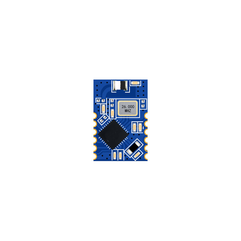
A Bluetooth module is only as good as the PCB it sits on. You can buy a pre-certified module with -95 dBm sensitivity and +8 dBm output, mount it on a carrier board with a sloppy ground plane and a 3 cm RF feed line through a via forest, and watch your effective range drop from 100 meters to 15. The module isn’t broken—your layout is.
This article covers the physical design rules that separate working BLE designs from problematic ones: RF feed line geometry, ground plane strategy, antenna keepout, decoupling topology, crystal placement, thermal management, and EMI mitigation. Every rule includes the numbers you need to implement it.
Module Placement: Start With the Antenna
The first layout decision is module placement, and it’s driven entirely by the antenna. Three module antenna configurations are common:
| Antenna Type | Keepout Required | Directionality | Placement Constraint |
|---|---|---|---|
| PCB trace antenna (on module) | 5 mm beyond module edge | Omnidirectional (with nulls) | Edge of carrier board, antenna end pointing out |
| Chip antenna (on module) | 3 mm beyond module edge | Quasi-omnidirectional | Edge preferred, less critical than trace |
| U.FL / MHF4 connector (external) | Minimal | Depends on external antenna | Connector at board edge for cable routing |
The rule is simple: the antenna end of the module goes at the edge of the carrier board, with no copper, no components, and no metal enclosure within the keepout zone. If you must place the module in the center of the board, use a module with a U.FL connector and an external antenna mounted on the enclosure.
Common placement mistakes:
- Module centered on board with PCB trace antenna → antenna radiates into ground plane, losing 10–15 dB
- Module near battery or metal shield → detuned antenna, shifted center frequency
- Module under display flex cable → absorption, 5–8 dB loss at 2.4 GHz
RF Feed Line Design: Coplanar Waveguide Math
If your module has a U.FL connector or an RF pad for an external antenna, you need an RF feed line on the carrier board. The standard choice is a grounded coplanar waveguide (GCPW), which provides good isolation and predictable impedance.
For a 4-layer FR-4 board (1.6 mm total, 0.3 mm prepreg between L1 and L2):
| Parameter | Value | Notes |
|---|---|---|
| Target impedance | 50 Ω | Standard for BLE modules |
| Signal trace width (W) | 0.50 mm (20 mil) | For GCPW on 0.3 mm dielectric |
| Gap to ground (G) | 0.20 mm (8 mil) | Tighter gap = more field confinement |
| L1 (signal) | 0.035 mm Cu | 1 oz copper |
| L2 (ground) | Solid plane | No splits under RF trace |
| Dielectric (prepreg) | 0.30 mm, εr ≈ 4.2 | Standard FR-4 at 2.4 GHz |
Verification: Using the Hammerstad-Jensen formula for GCPW, W=0.50 mm, G=0.20 mm, h=0.30 mm, εr=4.2, t=0.035 mm yields Z₀ ≈ 49.2 Ω—within 2% of target. If your board stackup differs, recalculate. Saturn PCB Toolkit or KiCad’s calculator handles this.
Critical Feed Line Rules
- Keep it short: Under 10 mm is ideal. Under 25 mm is acceptable. Over 50 mm introduces insertion loss (0.3–0.5 dB/cm at 2.4 GHz on FR-4) and acts as an antenna itself.
- No vias in the signal path: A via transition adds ~0.5 pF parasitic capacitance and creates an impedance discontinuity. Route the feed line entirely on L1. If a via is unavoidable, use a 0.2 mm via with 3 ground vias staggered around it.
- No right angles: Use 45° bends or curved traces. A 90° corner creates a parasitic capacitance bump of ~0.2 pF, causing a 0.3 dB reflection at 2.4 GHz.
- Ground stitching: Place ground vias (0.2 mm diameter) every 1.5 mm along both sides of the feed line, connecting L1 ground pour to L2 ground plane. This maintains GCPW impedance and prevents cavity resonance.
Ground Plane: The Foundation of RF Performance
The L2 ground plane directly beneath the module is the return path for all RF currents. Any discontinuity in this plane creates inductance, which shifts the module’s impedance match and degrades sensitivity.
Ground Plane Rules
- No splits: The L2 plane under and around the module must be solid. Route all signal traces on L3 or L4 if needed. A 2 mm split in the ground plane under a BLE module can shift the antenna resonance by 50–100 MHz.
- Module ground pads: Most modules have 3–6 ground pads. Connect every one to L2 with a dedicated via directly under the pad. Don’t share vias between ground pads—each pad needs its own low-inductance path.
- Ground via fence: Around the module perimeter, place 0.2 mm ground vias every 2 mm. This creates a Faraday cage that contains RF fields and prevents coupling to adjacent components.
Layer Stackup Recommendation
For a typical 4-layer carrier board:
Layer 1 (Top):    Signal + Component pads + RF feed line
Layer 2 (GND):    Solid ground plane (no splits, no signal routing)
Layer 3 (PWR):    Power plane + low-speed signals
Layer 4 (Bottom): Routing + ground pour
The L1-L2 prepreg thickness is the most critical dimension: it sets the GCPW impedance. Specify it explicitly in your fabrication notes (e.g., “L1-L2 dielectric: 0.30 mm ± 0.03 mm, εr 4.2 ± 0.2”). Don’t let the fab house choose the stackup.
Antenna Keepout: What Not to Put Near the Module
The antenna keepout zone extends beyond the module edge and must be free of conductive materials:
| Material | Minimum Distance from Antenna | Effect If Violated |
|---|---|---|
| Copper pour (any layer) | 5 mm | Detunes antenna, shifts freq 50–200 MHz |
| Components (caps, resistors) | 5 mm | Field absorption, 2–4 dB loss |
| Battery (CR2032, LiPo) | 10 mm | Significant absorption, 5–8 dB loss |
| LCD/display flex | 15 mm | Strong absorption + detune, 5–10 dB loss |
| Metal screws / standoffs | 5 mm | Local detune, pattern distortion |
| Metal enclosure wall | 10 mm (min) | Blocks radiation, use external antenna |
If your enclosure is metal and you can’t use an external antenna, the next best option is a plastic window in the enclosure above the module antenna. The window should be at least 15 × 15 mm and 1–2 mm thick ABS or polycarbonate.
Power Supply Layout: Clean Power Is RF Power
BLE modules draw current in sharp bursts: 8–15 mA during TX, 0.3 µA in sleep. The power supply must handle this transient without drooping or injecting noise into the RF path.
Decoupling Topology
Place decoupling capacitors in this order, closest to the module VDD pad:
- 100 nF X7R 0402: High-frequency decoupling. Place within 2 mm of VDD pad. This handles the 2.4 GHz switching harmonics.
- 1 µF X5R 0603: Mid-frequency decoupling. Place within 5 mm. Handles TX burst transients.
- 10 µF X5R 0805 or tantalum: Bulk decoupling. Place within 15 mm. Handles slow droop during sustained TX.
The 100 nF cap is the most critical. Its equivalent series inductance (ESL) must be under 1 nH. A 0402 X7R cap has ~0.7 nH ESL; a 0603 has ~1.2 nH. Always use 0402 for the high-frequency cap.
Power Trace Width
For a 1 oz copper, 0.3 mm dielectric:
- VDD trace: 0.30 mm (12 mil) minimum → handles 500 mA with 10°C rise
- For modules with PA boost (>10 dBm): 0.50 mm (20 mil) → handles 1 A peak
- Keep VDD trace on L1 or L3, never route under the module antenna
LDO vs DC-DC Selection
| Parameter | LDO (e.g., TPS702) | DC-DC (e.g., TPS62740) |
|---|---|---|
| Efficiency (3.7V→3.3V) | 89% | 95% |
| Output noise | 30 µV RMS | 500 µV RMS (with LC filter) |
| PSRR at 2.4 MHz | 45 dB | 20 dB (post-filter) |
| Quiescent current | 1 µA | 0.3 µA |
| Layout complexity | Low (3 components) | Medium (inductor + 4 caps) |
| Recommended for | Sensitive RX designs | Battery-powered, high drain |
If you use a DC-DC converter, add a second-stage LC filter (10 µH inductor + 4.7 µF cap) between the converter and the module VDD. This reduces switching noise to <100 µV RMS at the module, which is critical for achieving datasheet sensitivity.
Crystal Placement: Don’t Let It Drift
Most BLE modules have an integrated crystal, but some (bare IC packages like nRF52832 QFN) require an external 32 MHz crystal. Placement and load capacitance directly affect frequency accuracy, which affects BLE channel spacing compliance.
Crystal Layout Rules
- Distance from module: ≤ 3 mm. Longer traces add parasitic capacitance (0.1–0.2 pF per mm), shifting oscillation frequency.
- Trace symmetry: Both crystal pins should have equal trace lengths (within 0.2 mm). Asymmetry causes unequal parasitic capacitance, pulling the frequency off-center.
- Ground guard ring: Surround the crystal with a ground ring on L1, stitched to L2 with vias every 1 mm. This isolates the crystal from digital noise on adjacent traces.
- No signal traces under crystal: The L2 plane under the crystal should be solid ground. Route SPI, UART, and other signals away.
Load Capacitance Calculation
The load capacitance (CL) specified by the crystal manufacturer must match the total parasitic + explicit capacitance:
CL = (C1 × C2) / (C1 + C2) + Cstray

Where:
  C1, C2 = explicit load capacitors (typically equal, 8–12 pF)
  Cstray = PCB trace + pin capacitance (typically 2–5 pF)

Example: CL_spec = 12 pF, Cstray = 3 pF
  → C1 = C2 = 2 × (CL - Cstray) = 2 × 9 = 18 pF → use 18 pF
Wrong load capacitance causes frequency error. BLE channels are 2 MHz apart; a 40 ppm crystal error (±1.28 MHz at 32 MHz) puts you near the adjacent channel edge. If load capacitance is off by 2 pF, the frequency shifts by ~50 ppm—combined with crystal tolerance, you may fail BLE conformance.
Signal Integrity: Routing SPI, UART, and Debug
Module host interfaces (SPI, UART, SWD) operate at 1–8 MHz. While not as fast as DDR or PCIe, poor routing still causes issues—especially SPI, where clock skew causes data corruption.
SPI Routing (Up to 8 MHz)
- Trace length matching: MOSI, MISO, and CS should be within 5 mm of each other. Clock trace can be slightly longer (it’s the reference).
- Series termination: 22–33 Ω resistor on the clock line, placed within 10 mm of the module pin. This dampens overshoot/ringing on the clock edge.
- Ground return path: Route SPI signals over a continuous ground plane (L2). No splits or cutouts in the return path.
- Crosstalk: Keep SPI traces ≥ 2× trace width apart from each other and from other signals. At 8 MHz, crosstalk coupling is ~ -25 dB at 2× spacing.
UART Routing (Up to 1 Mbps)
UART is more forgiving than SPI—no clock line means no skew issue. Route TX and RX as a differential-ish pair (parallel, 0.2 mm apart) for cleaner return currents. Add a 100 nF cap on the UART RX pin if the trace is longer than 50 mm (prevents ESD coupling).
SWD Debug Port
Route SWDIO and SWCLK to a 0.1″ header or test pads. Keep traces under 30 mm. No series resistors needed—SWD is push-pull at low frequency (1–10 MHz during programming, idle during operation).
EMI and ESD: Protecting the Module
ESD Protection on Exposed Interfaces
Every pin that connects to the outside world (USB, buttons, external connectors) needs ESD protection:
- TVS diodes: Place at the connector, before any series resistance. Use low-capacitance types (≤ 1 pF) for high-speed signals (USB D+/D-, SPI clock). For UART and GPIO, 3 pF is acceptable.
- Series resistors: 100 Ω on button inputs, 33 Ω on UART lines. These limit ESD current before it reaches the TVS clamp.
- Ferrite beads: On power lines entering the board (USB VBUS, external power). Use 600 Ω @ 100 MHz, 0.5 A rated. Place at the connector.
EMI Mitigation
BLE modules themselves are low EMI emitters (the 2.4 GHz signal is contained within the module’s shield). The primary EMI sources are:
- DC-DC switching harmonics: A 2 MHz buck converter produces harmonics at 4, 6, 8 MHz… that can couple into the BLE receiver. Mitigation: LC filter on the output (10 µH + 4.7 µF), ground guard ring around the inductor, keep the switch node trace short and wide (it’s the primary radiator).
- SPI clock radiation: An 8 MHz SPI clock has significant energy at the 3rd harmonic (24 MHz). Route SPI traces on inner layers (L3) with ground above and below. If SPI must be on L1, add a ground via fence along the trace.
- USB D+/D- common-mode noise: Use a common-mode choke (e.g., TDK ACT45B-101-2P) on USB lines if USB is present. This reduces 30–300 MHz emissions by 10–15 dB.
Design Verification: Test Before You Build 10,000
Before committing to production:
RF Performance Verification
- Conducted TX power: Connect a spectrum analyzer to the U.FL test point (if available) or measure radiated power in an anechoic chamber. Verify output is within ±1 dB of the module datasheet spec.
- Conducted RX sensitivity: Use a signal generator at 2.402 MHz, GFSK modulation, 1 Mbps. Sweep input power from -90 to -100 dBm. Verify PER < 30.8% at the datasheet sensitivity spec.
- Antenna resonance: Measure return loss (S11) with a VNA. Target: S11 < -10 dB across 2.400–2.483 GHz. If the notch is shifted >50 MHz from center, adjust the antenna matching network or check the keepout zone.
Power Integrity Verification
- VDD ripple during TX burst: Measure with an oscilloscope (1× probe, 20 MHz BW limit) at the module VDD pad. Target: < 20 mV peak-to-peak during a BLE TX event. If higher, add more bulk capacitance or improve the LDO.
- Brownout detection: Monitor VDD during cold start (battery insertion). Some modules draw 15 mA surge current; if the supply droops below 1.7 V, the module resets. Add a 22 µF tantalum cap if this occurs.
Frequency Accuracy
- Measure the carrier frequency at 2.402 GHz (channel 37) with a spectrum analyzer. The center frequency should be within ±40 ppm of 2402 MHz (±96 kHz). If it’s off, check crystal load capacitance.
- Verify frequency across temperature (0°C to 50°C). AT-cut crystals have a parabolic temperature coefficient; expect ±20 ppm drift over this range.
Common Layout Review Checklist
Use this checklist during layout review before sending to fabrication:
- Module antenna at board edge, keepout zone clear on all layers
- L2 ground plane solid under module—no splits, no signal traces
- Every module ground pad has a dedicated via to L2
- Ground via fence around module perimeter (every 2 mm)
- RF feed line (if used) is GCPW, < 25 mm, no vias, no 90° bends
- 100 nF decoupling cap within 2 mm of VDD pad, 0402 package
- 1 µF cap within 5 mm, 10 µF bulk within 15 mm
- Crystal (if external) within 3 mm, symmetric traces, ground guard ring
- SPI series termination on clock line (22–33 Ω)
- ESD protection (TVS) on all external interfaces
- DC-DC switch node trace short and wide, LC filter on output
- No signal traces under module antenna keepout zone
- Board stackup explicitly specified (L1-L2 dielectric thickness critical)
A well-designed carrier board lets a Bluetooth module perform at its datasheet spec. A poorly designed one adds 5–15 dB of loss that no firmware patch can fix. Spend the time on layout review—it’s the cheapest way to improve RF performance.